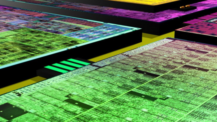
AMD has filed a patent describing a feature of the GPU chiplet design (multi-die). In particular, a new patent called Active Bridge Chiplet With Integrated Cache describes an active bus with integrated cache memory. We can assume that we are talking about the evolution of the Infinity Cache technology, which first appeared in the Radeon RX 6000 series video cards.
AMD’s idea is to assign to the interface connecting the individual GPU chiplets, including the role of L2 cache. Recall that in the current GPUs based on RDNA 3 architects, the Infinity Cache serves as the LXNUMX cache.
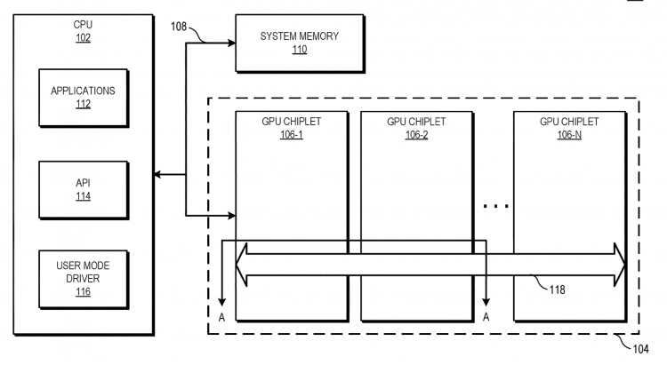
Block diagram showing a processing system using an active bus connecting GPU chiplets
AMD explains in the patent that any interaction between chiplets will be carried out through the active bus, which will be required to access memory channels on separate GPU crystals. Rather than relying on separate caches for each chiplet, AMD suggests using the active bus cache as a monolithic GPU cache. In other words, the cache memory will be addressed as a single registry.
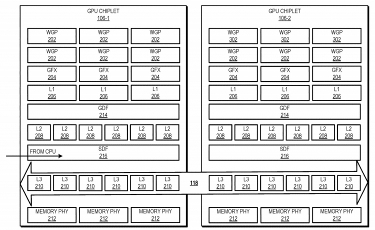
Block diagram of the cache memory hierarchy of GPU chiplets united by an active chiplet bus
AMD’s latest patent, like the previous one, which was reported in January this year, indicates that the company is actively investigating the use of multi-chip chiplet GPUs in the future. True, it is not yet clear whether we are talking only about new generation computational accelerators based on the CDNA architecture, or whether AMD is considering the possibility of using a chiplet design also in consumer video cards based on the RDNA architecture.
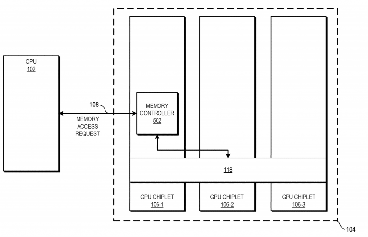
Flowchart for using a three-chip configuration
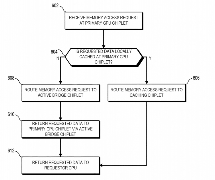
Diagram of the method of data exchange between chiplets
By the way, not only AMD is working in this direction. For example, Intel has a similar development and NVIDIA… The first has a huge multi-chip Xe-HPC, the second has GH100 (Hopper), which is also credited with multichip assembly (MCM).
If you notice an error, select it with the mouse and press CTRL + ENTER.