TSMC is the world’s largest contract chip manufacturer with nearly 500 customers. The company can serve almost any client with almost any requirement. At the same time, it must be ahead of all competitors, both in terms of capabilities and technology. The production volumes of TSMC are unlikely to be disputed by anyone in the coming years. In terms of mastering the advanced norms N2, N3 and N4, the company is also going according to plan.
TSMC significantly increased its 2021 capex budget earlier this year to $ 25-28 billion, and has now increased it further to about $ 30 billion as part of its three-year plan to spend $ 100 billion on manufacturing, research and development.
About 80% of TSMC’s $ 30 billion budget this year will be spent on expanding capacities for advanced technologies such as 3nm, 4 / 5nm and 6 / 7nm. Analysts at China Renaissance Securities believe that most of the money allocated for advanced rates will be used to expand the N5’s capacity to 110-120 silicon wafers per month (WSPM) by the end of the year.

TSMC was the first company to begin high volume production (HVM) chips using N5 (5nm) technology in mid-2020. Initially, only two companies used these services – Apple and Huawei HiSilicon. Deliveries for the latter ended on September 14, leaving Apple with all of its cutting edge capacity. By now, more and more customers are ready to start printing chips according to N5 standards, so the implementation of this technical process is increasing. TSMC says more customers are planning to use technologies from the N5 family (including N5, N5P and N4) than expected just a few months ago.
The manufacturer predicts that by the end of 2021, N5 will bring it about 20% of all revenues from the production of silicon wafers. TSMC is seeing more interest from customers for 5nm and 3nm norms than there was for 7nm at a similar stage. The company expects demand for the N5 will only grow in the near future due to smartphones and high-performance solutions.
The interest in TSMC N5 is not surprising: analysts from China Renaissance have calculated that the process technology can offer about 170 million transistors per square millimeter (MTP / mm2) Are the highest density rates to date. For comparison: Samsung 5LPE boasts a density of about 125-130 MT / mm2, and Intel’s 10nm norm is about 100 MT / mm2.
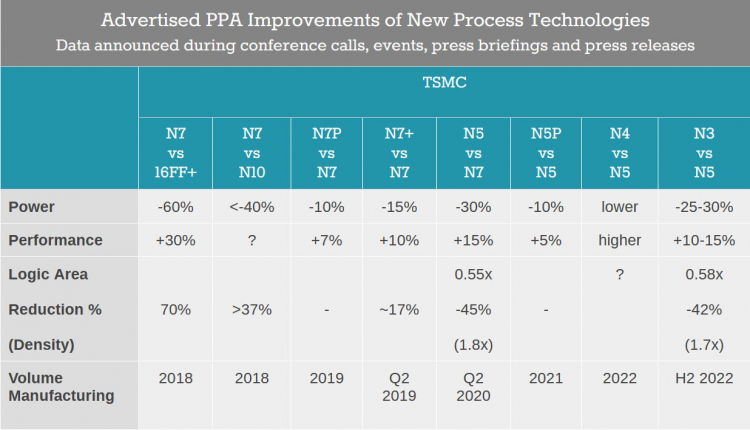
In the coming weeks, TSMC is set to begin manufacturing chips using an improved version of its 5nm technology called N5P, which promises to increase frequency by up to 5% or reduce power consumption by up to 10% (for the same crystal complexity). The technology does not require significant investment in engineering resources or longer design cycle times, so any TSMC customer who already has N5 chips can print with N5P.
TSMC’s N5 family of technologies also includes the N4 (4nm) process technology – with its help, the first chips will begin printing later this year, with mass production expected in 2022. This technology is intended to provide additional benefits in terms of power consumption, performance and density over the N5, while maintaining the same design principles, design infrastructure, and SPICE simulations. Meanwhile, as the N4 expands the use of extreme ultraviolet (EUV) lithography tools further, it will reduce the number of masking layers, production steps, and therefore risks and costs.
In 2022, the world’s largest contract chip manufacturer will also launch its completely new manufacturing process – N3 (3 nm), which will continue to use FinFET transistors. Compared to the current N5 process technology, it promises to increase performance by 10-15% (at the same power and complexity) or a decrease in power consumption by 25-30% (at the same frequency and complexity). The new regulations will also increase the density of transistors by 1,1 to 1,7 times depending on the structure (1,1X for analog, 1,2X for SRAM, 1,7X for logic).
N3 will further increase the number of EUV layers, but will still continue to use DUV lithography. In addition, as the technology will continue to use FinFETs, it will not require a new generation of electronic design automation (EDA) tools redesigned from the ground up and the development of entirely new chips, which could be a competitive advantage over 3GAE burs based on GAAFET / MBCFETs from Samsung. Risky production is scheduled for 2021, and mass production for the second half of 2022.
The structure of GAAFET (gate-all-around FET) transistors is still in the development plans of TSMC. It is expected that the company will use the new kind of transistors in the next important process technology after N3 (presumably N2, 2 nm). Notably, TSMC is expanding R&D capabilities at Fab 12, where work is currently underway on N3, N2 and more advanced manufacturing processes.

If you notice an error, select it with the mouse and press CTRL + ENTER.