3D NAND flash memory technology has almost reached 200 layers per chip. Due to the vertical layout, it was possible to combine high recording density, many rewrite cycles, small die sizes and the affordable cost of flash memory. The number of 3D NAND layers can be increased up to five times, but sooner or later the technology will hit a barrier. This will again force to reduce the size of memory cells with all the ensuing problems, but there is a way out.
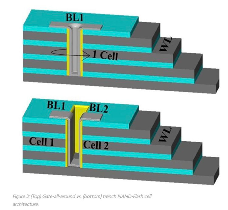
Image Source: IMEC
Recall that before the transition to the production processes for the production of NAND flash memory of the 10-nm class, memory was produced in the form of horizontal arrays (planar memory). But with the transition to 20-15-nm production standards, the volume of the cell decreased so much that the number of electrons in the volume of the cell material became tritely small for reliable charge retention. As a result, the number of erasing cycles decreased to several tens, and other electrical characteristics of the memory also deteriorated.
During this period, 3D NAND memory came to the rescue. The planar cell with all its structures was turned from a horizontal position and oriented to a vertical one. Thus, the area of the crystal on the plate was saved (read – the cost), and the memory capacity could be increased due to new layers up to 24, 32, 64, 128, 176 and more, as in the latest advanced 3D NAND chips. Due to the transition to a vertical arrangement of cells, their sizes increased significantly – up to 30–50 nm – with a step between cells up to 140 nm. This was enough to increase the resistance to wear without sacrifice for further increasing the recording density.
But in the future, with the transition to the production of 3D NAND with 500 or more layers, technological difficulties will increase, experts at the Belgian IMEC center believe . Therefore, it makes sense to reduce the size of already vertically arranged memory cells in order to increase the density of 3D NAND memory without increasing the number of layers. This can be done by dividing the vertical memory channels in two and at the same time by switching from a round channel profile to a rectangular one (elongated or, otherwise, trench).
In modern 3D NAND memory, the shutter covers the annular vertical channel from all sides. The transition to a rectangular channel will allow the gate to be divided into two independent ones and, therefore, will create two separate cells in the layer around the channel. The rectangular (trench) shape of the channel will ensure that the volume of the cell does not suffer much in this case. The electrical characteristics of the memory will deteriorate somewhat, but only slightly, and the recording density will increase sharply without significant complication of the production technology.
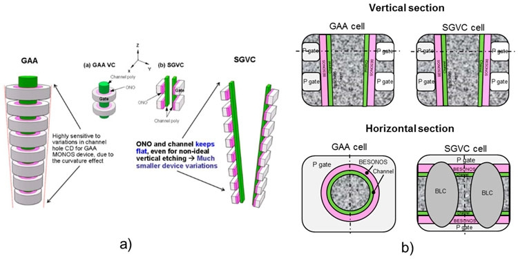
Relative comparison of 3D NAND with GAA and SGVC gates. Image Source: Macronix
Something similar was once offered by the Taiwanese company Macronix. Like IMEC, it divided the vertical channels into two independent structures, each of which worked with its own cells. Probably for this development, Toshiba later paid compensation to Macronix.
IMEC believes that the transition to a trench form of cells in 3D NAND memory will reduce the step between cells to 30 nm from the current 140 nm. This is the margin that will allow us not to sacrifice the volume of each vertical cell if they are divided into two in each layer. And this will also allow you to increase the recording density up to two times without increasing the number of vertical layers in 3D NAND memory.
If you notice an error, select it with the mouse and press CTRL + ENTER.


