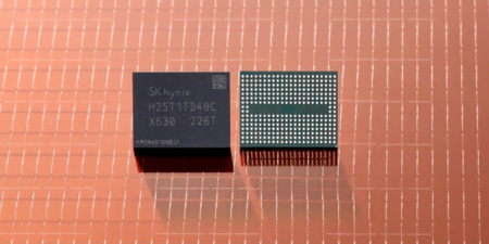
SK hynix has announced that it has developed the world’s first 238-layer 512Gb TLC 4D NAND memory chips. It is noteworthy that the latest 238-layer solution is both the most multilayer and the smallest in area.

Due to the small size, the overall manufacturing productivity increased by 34% compared to 176-layer NAND memory, since more chips with higher density per unit area can be produced from each wafer.
The data transfer rate of the 238-layer chip is 2.4Gbps, which is 50% faster than the previous generation. At the same time, the amount of energy consumed for reading data decreased by 21%.
SK hynix has already begun providing samples of 238-layer TLC 4D NAND memory chips with a capacity of 512 Gbps to customers. They will first be applied to client SSDs, followed by smartphone and high-capacity SSD solutions for servers. Next year, the company will also introduce 238-layer 1Tb chips, which will double the storage density of current 512Gb devices.
Well
QA evening
Learn for free, earn $700 at the start of the career
REGISTER!

Source: videocardz


