This year, the 68th annual IEEE International Electron Devices Meeting (IEDM) is back in full force, gathering nearly 1,500 engineers from around the world in person in San Francisco.
Among many materials of an academic and applied nature related to the development of the industry, TSMC’s report on the further perspective of scaling the density of SRAM cache memory made the greatest resonance. In short, it stopped. While the system logic of the processors still has a margin of scaling, the technologies used in industry are no longer able to significantly increase the density of SRAM.
At the conference, TSMC revealed its original N3B base node and an improved version of the N3E. Interestingly, for the new N3E node, the size of the high-density SRAM bit cell has not decreased at all. The area of the bit cell is 0.021 μm² – exactly the same as the N5 node. The N3B variant, which is not expected to be used by most products, has a smaller SRAM cell, but its 0.0199 µm² is only a 5% reduction compared to the N5 process. Regarding the approximate memory density, for the N3E it is approximately 31.8 MB/mm² and can increase to 33.55 MB/mm² or 1.75 MB/mm².
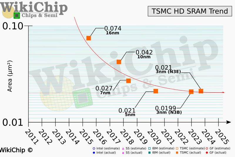
To visualize the pace and capabilities of processor development in perspective, note that while N3B and N3E provide 1.6x and 1.7x scaling of transistors only at the chip level, SRAM scaling is only 1-1.05 times. As before, you can expect TSMC to continue making denser SRAM bit cells for the N3, but there won’t be any major changes along the way.
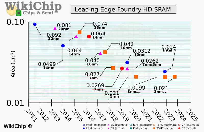
The SRAM scaling slowdown is not limited to TSMC, the problem has been around for quite some time. Intel is still able to reduce the density of SRAM cells, but recently in the recently announced Intel 4 process, SRAM scaling has slowed down to 0.7-0.8 times.
Impact of SRAM Scaling Stall on Processor Design
Currently, the only viable alternative to SRAM scaling is to increase the amount of cache memory – SRAM is expected to take up more space on the microchip die. This can increase the cost of manufacturing processors and prevent some architectures from becoming as small as they could be. The physical limitation of cache scaling becomes a factor that significantly affects the development of future architectures.
Most processors rely on cache memory as a high-speed data storage solution with minimal access time due to its strategic location next to the computing cores. Having fast and available storage can significantly improve processing performance and reduce the time spent by the cores to do their work. Accordingly, the slowdown in the development of caching technology imposes limitations on the growth of performance.
Future prospects and alternatives for improving cache memory
Some research institutes such as Imec have already introduced higher density SRAM cells. Last year at IEDM 2021, Imec demonstrated an SRAM density of around 60MBmm², roughly double today’s density on a hypothetical node above 2nm – using branched transistors and an advanced two-way interconnect scheme.
In addition to SRAM, the industry is exploring many other alternative memory architectures. Among them are MRAM, FeRAM, NRAM, RRAM, STT-RAM, PCM and other technologies. These new bit memory cells offer unique tradeoffs compared to SRAM, such as higher density with lower read/write performance, non-volatile capabilities, faster read-write cycles, or lower power consumption.
Although these technologies are not a direct replacement for SRAM, in the future it will be possible to create cache memory of the fourth or fifth levels based on them, in which the decrease in performance can be compensated by higher density.
DigiTimes: TSMC to sell 3nm wafers for $20,000 — 25% more than 5nm wafers
Sources: WikiChip Fuse, TechSpot