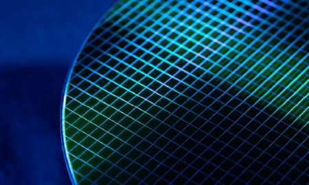
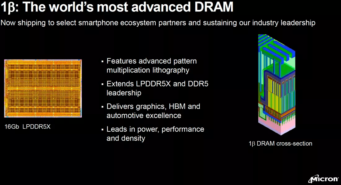
Micron is sending out prototypes of what it claims is the world’s most advanced DRAM technology. After the mass delivery of 1-alpha in 2021, the new 1-beta LPDDR5X is supposedly better in almost every way. According to Micron, the node is about 15% more power efficient and provides over 35% improvement in bit density at 16Gb per die.
Micron CEO Scott DeBoer said the technology is brought to life by the company’s patented multi-pattern lithography process, combined with advanced manufacturing processes and materials. With a new lithography process, Micron was able to bypass the extreme ultraviolet radiation (EUV) technology that manufacturers have been using lately.
Mobile devices will be the first to take advantage of Micron’s new technology. Artificial intelligence and other data-intensive programs will be able to use the increased bandwidth more efficiently. Even basic apps like the camera will benefit from reduced startup times and improved performance in night and portrait modes. RAM that requires less power will result in longer battery life.
Micron has also implemented new JEDEC Advanced Dynamic Voltage and Frequency Scaling (eDVFSC) methods. According to the company, the addition of eDVFSC provides up to 3200 Mbps (1600 Mbps in the 1-alpha version).
Last month, Micron announced plans to spend up to $100 billion over the next two decades to build a world-class semiconductor manufacturing plant in upstate New York. This is the largest private investment in New York history. The recently passed CHIPS Act paved the way for Micron to build in the US rather than abroad.
Micron said it plans to grow its 1-beta product portfolio over the next year, including consumer, consumer, industrial, embedded, automotive and data center segments.
Unfair advantage for Intel – the US semiconductor industry is divided due to incentives in the CHIPS Act and FABS
Source: tech spot