TSMC has outlined plans to put more than 1 trillion transistors in 3D packaging and 200 billion in monolithic chips by 2030. At the IEDM 2023 conference, the company revealed a roadmap for what its semiconductor portfolio should look like, and it looks like the Taiwanese giant has ambitious plans for the end of this decade.
Based on the released roadmap, TSMC is confident that its processes are on the right track: TSMC’s N2 and N2P processes will debut in 2025-2027, and the advanced A10 (1nm) and A14 (1.4nm) processes are scheduled for 202030 year. In addition to reducing technological processes, TSMC plans to achieve significant progress in other semiconductor technologies, setting benchmarks for the industry, Wccftech reports.
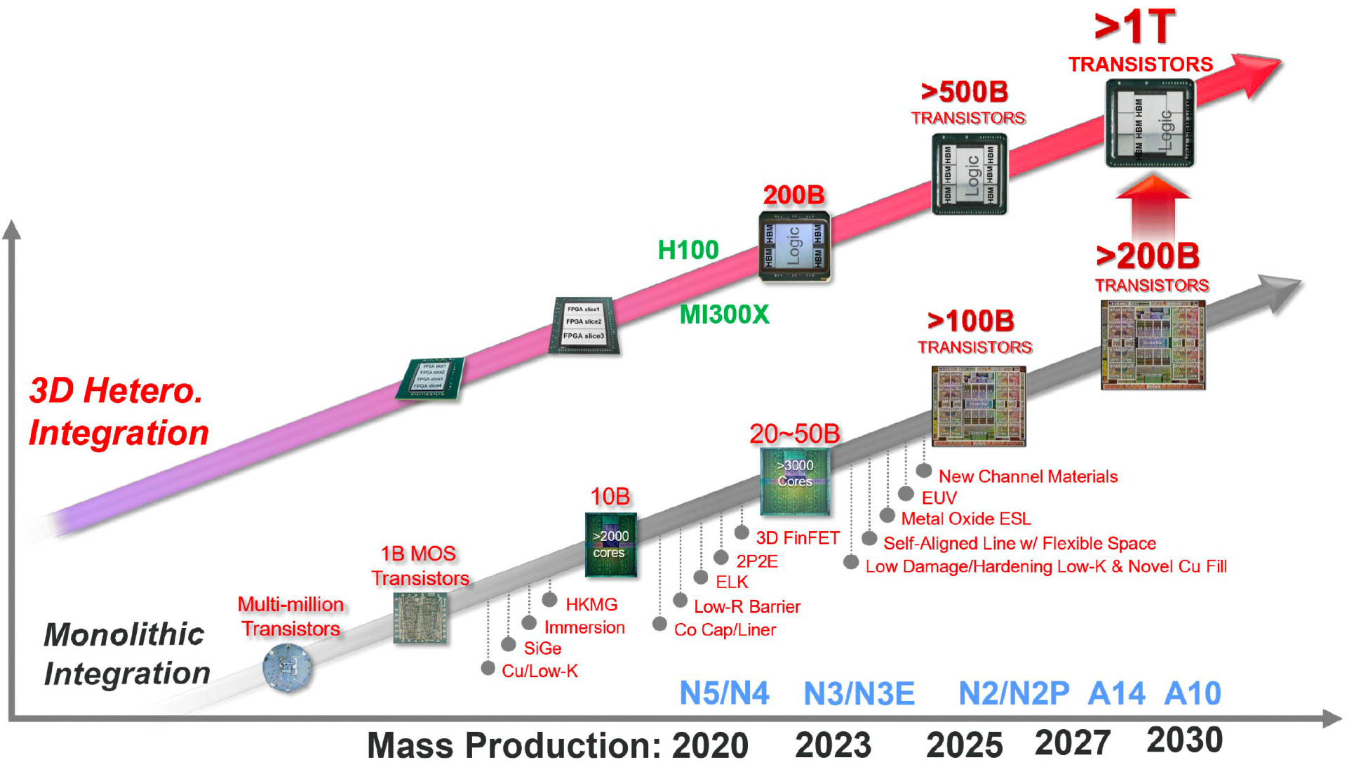
More interestingly, the Taiwanese giant revealed advances in two key sectors of the semiconductor industry – monolithic structures and 3D heterointegration (or chiplet structures). The industry is really shifting towards chiplet configurations because they offer modularity and cost-effectiveness.
AMD is using TSMC chip designs for new consumer chips, data center chips, and now the latest MI300 accelerator chips. Intel also released its Meteor Lake, the blue team’s first development for consumer platforms, hinting that the future is chiplets and TSMC is one step ahead. Intel itself uses TSMC processes for Meteor Lake. The company predicts that by 2030, 3D heterointegration will reach the colossal volume of “one trillion transistors.”