South Korean company Samsung Electronics is accelerating the launch of its third semiconductor factory in the Korean city of Pyeongtaek. Reported by the Korean edition Press, citing industry sources.
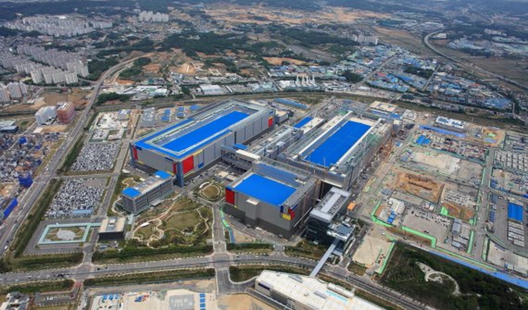
According to one source, the company has already ordered production equipment for the new line. Its specifics indicate that Samsung will produce on the P3 DRAM chips based on 10nm process technology using EUV lithography to increase production per wafer, as well as seventh generation 3D V-NAND flash memory chips with 176 or more layers. … It is indicated that the supply of equipment is expected by the completion of construction work, namely in the spring of next year.
The groundbreaking of the P3 plant began in September 2020, when the semiconductor industry crisis was just brewing. Experts estimate that Samsung could spend $ 26,7 billion to $ 44,3 billion on new production when it reaches full capacity by 2023.
According to the source, the company has not yet decided whether the new enterprise will produce semiconductor products under contract orders from third-party companies. This decision is likely to depend on the potential scale of such orders.
It is also indicated that Samsung has already formed a design team for the P3 line. The company planned to share details about the project back in January this year, but postponed this decision. This is attributed to the fact that on January 18, the CEO and de facto leader of the Korean giant Lee Jae-yong was sentenced to two years and six months in prison on bribery charges.
If you notice an error, select it with the mouse and press CTRL + ENTER.