Researchers from TSMC with colleagues from the United States and the National Taiwan University presented a work on transistors made of so-called 2D materials that can replace silicon electronics. In a joint study, experts have found such a combination of materials that makes it possible to produce transistors from materials with a thickness of one or more atoms. The discovery may well form the basis of TSMC’s 1nm process technology.
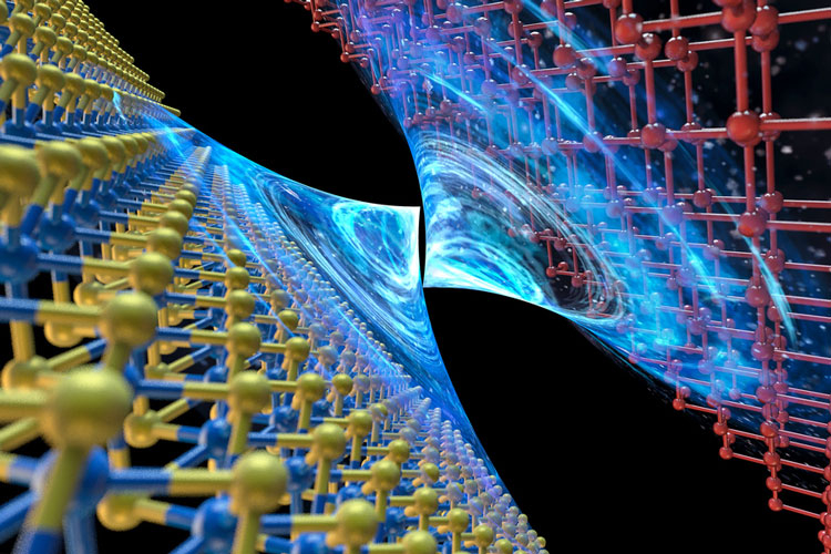
The problem with 2D materials is that the contact point between the semiconductor and the metal has high resistance and degrades the current characteristics of transistors. Researchers from the Massachusetts Institute of Technology, the University of California at Berkeley, TSMC, the National Taiwan University and several other organizations were able to choose the right combination of materials that provided all the necessary characteristics of “two-dimensional” transistors.
Everything turned out to be simple. A decrease in resistance at the interface between a two-dimensional semiconductor represented by molybdenum sulfide (MoS2) and a metal contact for connection with other circuits of the electronic circuit occurred when the material came into contact with the semimetal bismuth (Bi). At the interface between the materials, as scientists say, there was no energy barrier (Schottky barrier) that could prevent the free passage of electrons – the flow of electric current.
From this study, it was concluded that the electrical contact between MoS2 and Bi is a perfectly working solution for creating an n-type transistor. Researchers do not yet have solutions for creating a similar p-type transistor, so there is still no way to create a full-fledged electronic circuit from 2D materials. But the search for promising combinations of materials will not stop there, so everything is still ahead.
The main scientific search was carried out by scientists from the United States. TSMC was able to create contact patterns on its equipment by vapor deposition in a vacuum chamber. Scientists from the National Taiwan University helped to create the necessary basis for etching on a crystal, who were able to focus an ion beam to the nanometer scale. The study is funded by the US Department of Defense. Ultralow contact resistance between semimetal and monolayer semiconductors was published in Nature.
If you notice an error, select it with the mouse and press CTRL + ENTER.