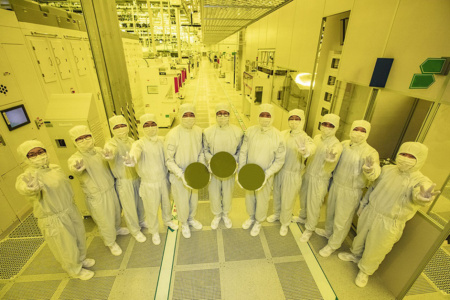
Samsung Electronics has announced the start of manufacturing chips based on its 3nm process node using the Gate-All-Around (GAA) transistor architecture.

Note that the GAAFET architecture, which replaces the current FinFET, has been developed by an organization that includes IBM, Globalfoundries and Samsung since 2000. It should help overcome the physical limitations of MOS scaling. The main feature of GAAFETs is ring gates (hence the name gate-all-around FET). The channels of GAAFET transistors are nanowires (they are formed from several horizontal silicon “nanosheets”). At the same time, the channel of the FinFET transistor under the gate is a monolithic vertical “fin” structure, which imposes scaling restrictions.
Samsung has its own implementation of GAAFET technology, which is marketed as Multi-Bridge-Channel FET (MBCFET). In fact, MBCFET differs from GAAFET not only in name, but also technically: in the case of Samsung implementation, the channels are made in the form of flat “bridges” rather than “wires”.
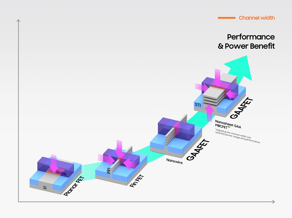
According to Samsung, MBCFET technology overcomes the performance limitations of FinFET, improving power efficiency by lowering the supply voltage level, and improving performance by increasing the drive current capability. Samsung’s proprietary technology uses nanosheets with wider channels, resulting in higher performance and greater energy efficiency than GAA technologies using narrower channel nanowires. Using 3nm GAA technology, Samsung will be able to adjust the nanosheet’s channel width to optimize power consumption and performance to meet different customer needs.
The new technology will be used to produce semiconductor chips for low-power, high-performance computing applications and also plans to expand it to mobile processors.
It is noted that the optimized 3nm process technology provides a 45% reduction in power consumption, a 23% increase in performance, as well as a smaller die area by 16% compared to the 5nm process technology.
Additionally, Samsung announces 3nm design infrastructure and services with SAFE (Samsung Advanced Foundry Ecosystem) partners including Ansys, Cadence, Siemens and Synopsys. This should help customers improve their product in the shortest possible time.
Source: videocardz