This week, Western Digital revealed its 3D NAND memory development plans for the coming years. Among other things, the company noted that, together with its partner Japanese company Kioxia, it is developing 162-layer flash memory chips with a reduced cell area and high-performance flash memory with more than 200 layers.
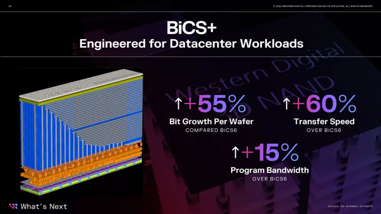
Image Source: Western Digital
Next-generation 3D NAND memory BiCS6 will appear towards the end of this year. At first glance, these will not be the most advanced chips in terms of the number of vertical layers – only 162 layers, which looks quite modest against the background of the 232-layer 3D NAND chips just introduced by Micron. However, the capacity of WD and Micron solutions is the same – 128 GB (1 Tbit). And the area of BiCS6 will be the most compact in the industry 68 mm 2 . The company was able to achieve this by significantly reducing the physical size of the memory cells, which was helped by the use of a new material in their structure.
In addition, the BiCS6 memory will store four bits in each cell (QLC). Reducing the physical size of the cell with a combination of writing four bits to each of them should lead to a decrease in the number of rewrite cycles, but WD has not yet disclosed this value. At the same time, the speed of BiCS6 memory promises to be 60% higher than in the case of modern solutions, which will allow it to be used both for the production of mass drives and capacious server SSDs. Increasing the density should also reduce the cost of production, which is important for everyone.
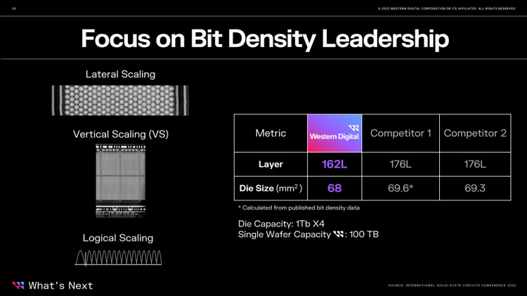
Image Source: Western Digital
Another new development looks no less interesting – BiCS + memory with more than 200 layers. It is claimed that it is being developed from scratch primarily for server-side SSDs. BiCS+ memory will appear by 2024 and will provide up to 55% more bits per platter compared to BiCS6 memory, as well as a 60% increase in speed. Also, the write speed will increase by 15%, which is no less important for NAND flash memory than everything else.
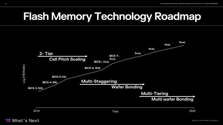
Image Source: Western Digital
Going forward, WD, like other 3D NAND vendors, is aiming for 500 or more 3D NAND layers. Such memory can only be produced using a combination of many technologies, including vertical “gluing” of memory crystals. The company does not lose hope of releasing memory with five bits per cell (PLC), but it is no less difficult than releasing 3D NAND with 500 layers, which delays the time of its appearance.
If you notice an error, select it with the mouse and press CTRL + ENTER.