At the Intel Unleashed: Engineering the Future event, Intel CEO Pat Gelsinger spoke about the implementation of a project to develop the Ponte Vecchio accelerator designed for use in high performance computing (HPC) systems.
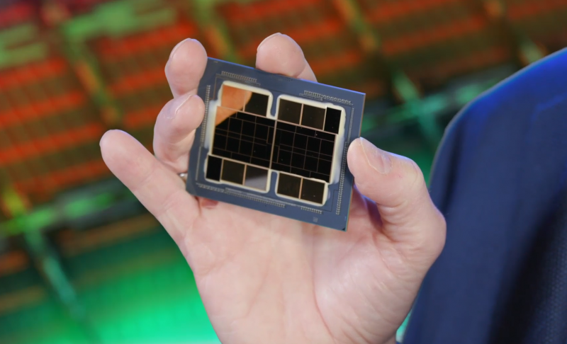
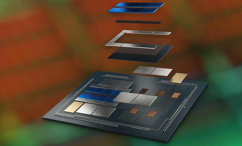
It is noted that in a little more than two years of the project’s existence, Intel specialists managed to achieve outstanding results. In particular, a prototype working processor has already been created. Mr. Gelsinger showed such a product during his speech. The processor has a “tiled” design with 47 elements, which is clearly visible in the published images.
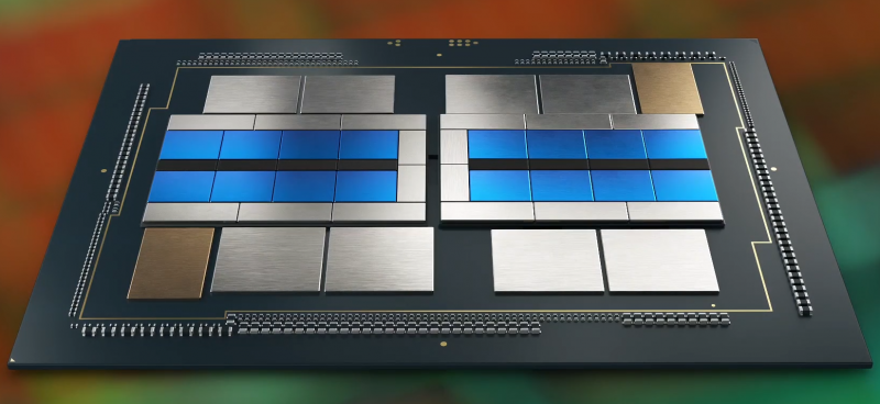
Manufacturing uses both Foveros 3D layout and EMIB connections. The total number of used transistors exceeds 100 billion. It is also reported that the solution provides performance in excess of one petaflops. But it is not specified what kind of accuracy we are talking about.
For comparison: AMD MI100 has a peak FP64 performance of 11,5 Teraflops (and twice as much for FP32), while NVIDIA A100 has 9,7 Teraflops for FP64 and 19,5 Teraflops for FP32. For other formats (bfloat16, FP16, INT4 or INT8) these values are many times higher for both accelerators.
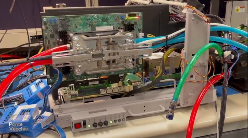
Ponte Vecchio GPUs will be used in tandem with Xeon processors codenamed Sapphire Rapids. Ponte Vecchio solutions, in particular, will be part of the Aurora supercomputer for the US Department of Energy’s Argonne National Laboratory. It is planned to complete the creation of this system by the end of this year.
If you notice an error, select it with the mouse and press CTRL + ENTER. | Can you write better? We are always glad to new authors.
A source: