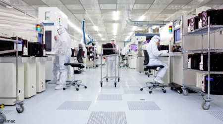
IMEC has revealed the details of the roadmap for technological nodes that await us until 2036. The presentation was held at the Future Summit in Antwerp (Belgium).

A research company has prepared a report that talks about the use of nodes in advanced semiconductors (CPU, GPU, SOC, etc.), revealing what awaits us beyond 1 nm.
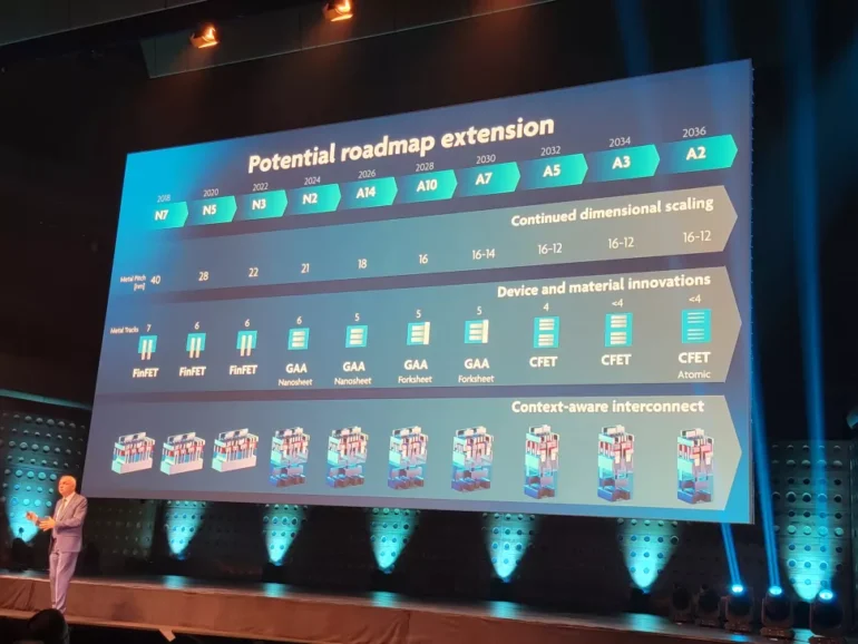
The roadmap includes FinFET transistors that will operate down to 3nm, to new Gate All Around (GAA) nanosheets, and forksheet designs from 2nm to A7 (seven angstroms).
Starting from 1 nm, the nodes of the process begin to be measured by “angstroms”. 10 angstroms equals 1nm, so nodes smaller than 1nm will ship with the A7. This will happen from 2030.
Gate All Around (GAA)/Nanosheet transistors will debut in 2024 with a 2nm node, replacing the FinFETs used in today’s advanced chips. Intel has already shown four-leaf RibbonFET chips that use variations of this transistor technology.
Multi-patterns (more than one exposure per layer) can be used on 4th generation EUV lithographic machines with 0.33 aperture to create chips at 2nm and above. But reprinting a single layer increases the chance of defects, resulting in lower productivity, higher production and higher costs.
Fifth-generation machines with 0.55 aperture will be able to create smaller structures in a single exposure, increasing production rates to over 200 plates per hour. Such tools for mass production will appear as early as 2026, and the first high-aperture lithographic machine will be completed in the first half of 2023. ASML spent $400 million to create it.
IMEC expects GAA/nanosheet and forksheet transistors to be used down to A7 nodes (less than 1nm). Until 2032, complementary field-effect transistors (CFETs) will be used, and by 2036, the firm expects atomic-channel CFETs to be used.
The ability to increase transistor density and reduce node size will be critical to improving computing performance and adding new features. Further increases in transistor density will require advanced Back End of Line (BEOL) processes. They focus on connecting transistors together, providing both communication (signals) and power delivery.
IMEC refers to these methods of increasing secondary density as “scaling amplifiers” because they tend to increase transistor density and performance, even though they are not directly related to transistor size/placement.
IMEC believes that Moore’s law will continue to hold true, which will be a problem for the entire industry, especially with the advent of machine learning. As nodes develop, the demand for electricity increases and costs increase dramatically. Magnetic gates could be an alternative as the industry moves inexorably towards quantum computing.
The European Commission approved the “Law on chips” – with investments of more than 43 billion euros to expand the production of semiconductors